

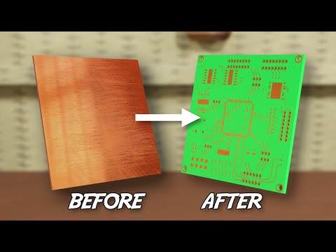
Printed Circuit Boards (PCBs) are the unsung, unknown heroes that power our modern world, from smartphones and laptops to intricate medical devices and aerospace systems.
At the heart of these electronic marvels lies a meticulously orchestrated process known as PCB assembly. In this article, we will take you on a journey through the fascinating world of PCB assembly, shedding light on the steps involved, the critical considerations, and what you should know about this pivotal aspect of electronics manufacturing.
The journey begins with design. Engineers and designers collaborate to create a blueprint for the PCB layout, defining the circuit’s functionality, component placement, and routing of electrical traces. Prototyping often follows, allowing for testing and refinement to ensure the design meets specifications. Design software and simulation tools are crucial in this phase, enabling precise planning.
Quality is paramount in PCB assembly, and selecting the right materials is crucial. PCB manufacturers carefully source high-quality substrates, copper foil, and solder mask materials to ensure optimal performance and durability. These materials often adhere to industry standards and regulations.
The PCB fabrication process involves transferring the design onto a substrate using chemical etching and mechanical drilling. This process creates the copper traces, vias, and pads necessary for electronic connections. Advanced techniques like multilayer PCB fabrication are employed for complex circuits, where multiple layers are bonded together.
Sourcing electronic components is a critical step. Manufacturers collaborate with a network of suppliers to procure various components, including resistors, capacitors, integrated circuits, and connectors. These components’ compatibility, quality, and availability are carefully considered to ensure seamless assembly.
Solder paste, a critical element in PCB assembly, is applied to the board using a stencil. This paste, a mixture of tiny solder particles and flux, allows components to be temporarily held in place before the final soldering process. Precision in applying the solder paste is essential to prevent defects.
In the pick-and-place phase, automated machines meticulously position surface-mount components on the PCB using the solder paste as an adhesive. These machines operate incredibly quickly and precisely, placing thousands of components per hour.
The heart of the assembly process is reflow soldering, where the PCB is subjected to controlled heating, causing the solder paste to melt and form secure electrical connections. The temperature and duration of the reflow process are carefully monitored to prevent damage to sensitive components.
After soldering, a thorough inspection is carried out. Automated optical inspection (AOI) and X-ray testing detect defects, such as solder bridges or misaligned components. Any issues are corrected before proceeding.
Functional testing is the final step, where the assembled PCB undergoes a series of tests to ensure it operates as intended. This phase verifies that all components work correctly and that the circuit functions according to design specifications.
In the grand orchestra of technological advancements, PCB assembly conducts a symphony, orchestrating electronic marvels with precision and harmony. Imagine, if you will, each component as a musician, each circuit trace as a melody, and the entire PCB as a symphonic masterpiece. The conductor, our skilled engineers, ensures each element plays in harmony, creating a melody that powers our digital world. Isn’t it fascinating how these unseen maestros, the PCBs, silently compose the rhythm of our technological lives, from the gentle hum of a computer to the vibrant resonance of a smartphone?
PCB assembly is not merely a process; it’s an art form where science and creativity intertwine. Picture an artist, palette in hand, meticulously placing each component, each resistor, and capacitor, as strokes of color, crafting a masterpiece that is not only functional but also efficient. The canvas, the PCB, holds the potential to bring forth innovations, much like how a blank canvas can birth a timeless painting. How often do we pause to appreciate this blend of art and science that quietly propels our digital experiences?
Have you ever pondered PCBs’ silent, pivotal role in our technological tales? They are the unsung heroes, diligently channeling electrons, ensuring our devices spring to life, and our communications traverse continents in seconds. In the epic of modern technology, PCBs may not bask in the limelight, yet their role is undeniably central. They are the hidden protagonists, ensuring the plot of our digital narratives unfolds seamlessly, connecting tales of innovation, communication, and progress.
Embark on a journey from a mere blueprint to a fully functional electronic device, where each step in PCB assembly is a milestone towards technological marvels. The path, while intricate, is paved with precision, expertise, and a dash of innovation. It’s a journey where ideas morph into reality, concepts take a tangible form, and innovations are envisioned and realized. Can we ever truly grasp the depth of expertise and meticulousness encapsulated in this journey from conception to electronic functionality?
We find a bridge connecting our technological past with an innovative future in PCB assembly. It’s a bridge constructed with traces of copper, components, and a wealth of knowledge. As we traverse this bridge, we carry forward the wisdom from past innovations while reaching toward the future’s untapped potential. How does this bridge, so intricately woven with circuits and components, ensure that the legacy of past technologies is seamlessly melded into the future’s innovations?
The PCB assembly process is a complex and precise endeavor in which science, technology, and craftsmanship combine to create the electronic devices that define our modern lives. Understanding the intricacies of this process empowers us to appreciate the depth of engineering and expertise that goes into each PCB, whether it’s in our pocket-sized smartphones or the advanced technology propelling space exploration. PCB assembly is not just a manufacturing process; it’s a testament to human innovation and the foundation of our interconnected digital world.
What is the significance of PCB assembly in our digital world?
PCB assembly is crucial as it orchestrates the functionality of electronic devices, ensuring each component works in harmony to power our digital experiences, from everyday gadgets to advanced technological systems.
How does PCB assembly blend art and science?
PCB assembly intertwines art and science by meticulously placing each component, much like strokes of color on a canvas, crafting a masterpiece that is functional and a testament to innovative engineering and creative problem-solving.
Why are PCBs considered the unsung heroes of technology?
While often unseen and uncelebrated, PCBs play a pivotal role in ensuring the seamless functionality of our electronic devices, silently powering our digital narratives and connecting tales of innovation, communication, and progress.
How does the PCB assembly process transform ideas into reality?
The PCB assembly process transforms ideas into reality by translating a conceptual blueprint into a tangible, functional electronic device, ensuring that innovative concepts take a physical form and become operational.
How do PCBs bridge the technological past and future?
PCBs act as a bridge between the technological past and the future by carrying forward the wisdom from past innovations and ensuring that the legacy of previous technologies is seamlessly integrated into future innovations, providing a platform for continual technological advancement.
What materials are typically used in PCB manufacturing?
High-quality substrates, copper foil, and solder mask materials are commonly used in PCB manufacturing to ensure optimal performance and durability, often adhering to industry standards and regulations.
What is the role of solder paste in PCB assembly?
Solder paste, a mixture of tiny solder particles and flux, is applied to the PCB to temporarily hold components in place before the final soldering process, ensuring precision and preventing defects.
How is quality ensured during PCB assembly?
Quality is ensured through various inspection and quality control steps, utilizing Automated Optical Inspection (AOI) and X-ray testing to detect defects like solder bridges or misaligned components, which are corrected before proceeding.
What is the purpose of functional testing in PCB assembly?
Functional testing verifies that the assembled PCB operates as intended, ensuring all components work correctly and the circuit functions according to design specifications, validating the assembly process’s success.
How does PCB assembly contribute to technological advancements?
PCB assembly plays a pivotal role in technological advancements by enabling the functionality of electronic devices, from everyday gadgets to complex aerospace systems, facilitating innovations and developments in various fields.
What are the challenges faced during PCB assembly?
Challenges in PCB assembly include ensuring precision in component placement, maintaining quality and consistency, managing material procurement, and adhering to industry standards and regulations.
How does PCB assembly
The cost of PCB assembly, which involves material procurement, manufacturing, and quality control processes, significantly impacts the overall cost of electronic devices, influencing their market price and accessibility.
What is the difference between SMT and Through-Hole mounting technologies in PCB assembly?
Surface Mount Technology (SMT) involves placing components directly onto the surface of the PCB. In contrast, Through-Hole mounting involves inserting component leads through holes in the PCB, each with distinct applications and assembly advantages.
How does PCB assembly adapt to advancements in electronic components?
PCB assembly adapts to advancements by incorporating new technologies, materials, and methods, ensuring compatibility with evolving electronic components and meeting the demands of new applications and innovations.
What is the role of engineers and designers in PCB assembly?
Engineers and designers collaborate to create the PCB layout, defining circuit functionality, component placement, and routing of electrical traces, ensuring the design meets specifications and adheres to industry standards.
How does PCB assembly accommodate the assembly of complex circuits?
Complex circuits, such as multilayer PCBs, are accommodated through advanced techniques like multilayer PCB fabrication, where multiple layers are bonded together to meet the requirements of intricate electronic applications.
What considerations are made during the component procurement step in PCB assembly?
During component procurement, considerations include the compatibility, quality, and availability of components like resistors, capacitors, and integrated circuits to ensure seamless assembly and optimal functionality.
How does PCB assembly ensure the durability and reliability of electronic devices?
Through meticulous material selection, precise assembly processes, and rigorous quality control and testing, PCB assembly ensures the durability and reliability of electronic devices across various applications.
What are the environmental considerations in PCB assembly?
Environmental considerations include adhering to regulations regarding material usage, managing waste and recycling processes, and ensuring energy-efficient manufacturing practices to minimize the ecological
How does PCB assembly support the functionality of smart devices?
PCB assembly supports smart devices by enabling the integration and functionality of various electronic components, facilitating communication, processing, and operational capabilities essential for smart technology applications.